The need for Quantum Communications
The rise of quantum computers will break public key cryptography and consequently render obsolete existing secure communication infrastructures our modern society relies upon. This imminent threat prompts development of new counter technologies, and one of the most promising candidates is quantum communication. Quantum physics provides the ideal background to work with, due to the inherent uncertainty of quantum properties. Such uncertainty is crucial to generate randomness, which is the main ingredient of secure communications.
Quantum Key Distribution
Quantum Key Distribution (QKD) is one of the several ideas which exploit quantum randomness. Generating an encryption key, shared between two parties and unknown to any attackers, is the goal of the different QKD protocols. The security of the generated key is guaranteed by the laws of quantum physics: an eavesdropper can not do better than just guess the encryption key, no matter their computational power.
The BB84 protocol was the very first QKD protocol, introducing for the first time the idea of using the quantum states of photons to distribute a key between two parties. After that, a myriad of new protocols were proposed, each with their own advantages and disadvantages. The underlying concept, however, remains unchanged: one of the two parties, Alice, sends the other, Bob, a random sequence of bits encoded in a quantum property of a train of photons (polarisation, phase, time); an eavesdropper intercepting the signal inevitably disturbs the quantum state and, consequently, introduces noise at the receiving end that will highlight the presence of eavesdropping.
Since that first proposal in 1984, QKD has attracted a great deal of interest in the scientific community. Its experimental implementations have improved substantially: the communication distance has risen from a mere 32cm in free space in the very first QKD experiment, to 421km of optical fibre in a recent demonstration. This impressive distance can even be extended much further with the newly discovered TF-QKD protocol (which will be covered in the next story of the month).
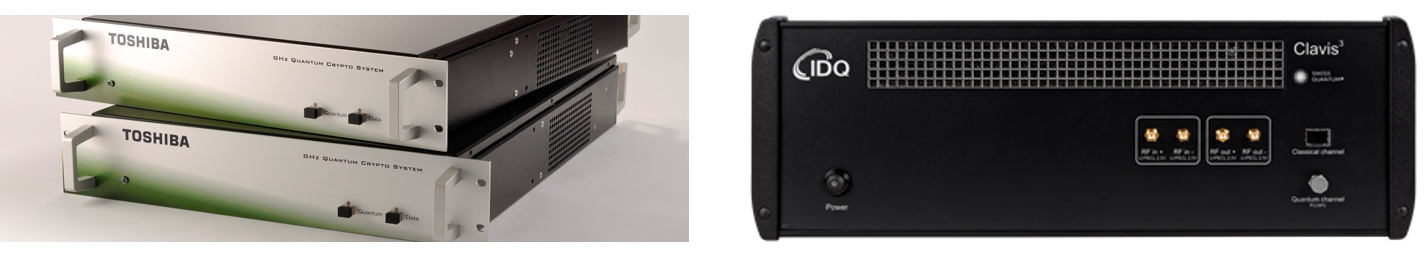
QKD has gained popularity outside academia as well, with companies like QCALL partners Toshiba and ID Quantique developing their own QKD systems.
Chip-based QKD
Large-scale deployment of QKD systems is yet to become a reality. One of the obstacles is that existing QKD equipment is space and power consuming, and very expensive.
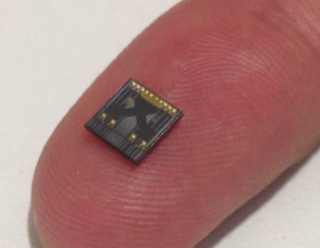
To mitigate these constraints and ease the QKD path to market, it is necessary to miniaturise and mass-produce the QKD devices. This is the main focus of QCALL project #1, aiming at the development of integrated photonic devices for Quantum Communications.
Integrated Photonics
Photonic Integrated Circuits (PICs) are already a widespread technology in classical communications. They have the capability of embedding a plethora of optical components on a very small form factor device.
In addition to this, mass production of photonic chips is significantly cheaper than assembling from discreet, bulky components, thanks to generic integration technology and multi-project wafers: like with electronic printed circuit boards, the foundries release a set of basic building blocks, which their clients will assemble to make their own circuits. This way, all components can be grown and processed on a wafer monolithically, i.e. in a single run: this allows for multiple circuits to be implemented at the same time, drastically lowering development and production costs for both the foundry and their clients.
Chip-based quantum communications
Integrated photonics seems the natural choice for nxet’generation Quantum Communications devices since their performance is well established in classical communications.
Among the building blocks needed for a QKD transmitter, there are lasers, waveguide couplers, phase modulators and photodiodes. All these can easily be implemented on a chip, and indeed there are several examples of chip-based devices implementing QKD protocols.
Our goal at Toshiba is to make smaller, cheaper and more efficient QKD devices based on photonic integration.
Chip-based quantum communications at Toshiba
Chip-based Quantum Random Number Generator
In order to correctly implement any QKD protocol, a prerequisite is that the initial bit sequence, sent from Alice to Bob, has to be truly random, otherwise an eavesdropper could exploit correlations among the bits to guess the bit sequence.
Generating true randomness is difficult and even fundamentally impossible by only classical means. The deterministic laws of electrodynamics always deliver a predictable outcome, in principle. However, the outcome becomes different in quantum physics. In our Quantum Random Number Generator (QRNG), we generate pulses from two independent laser and have them interfere on a beam splitter. The spontaneous emission process triggering the lasing action is of quantum nature. This guarantees that the phase of the optical pulses emitted by the lasers is inherently random. Hence, when the two pulses interfere, their interference amplitude is not predictable and we can use it to extract random numbers.
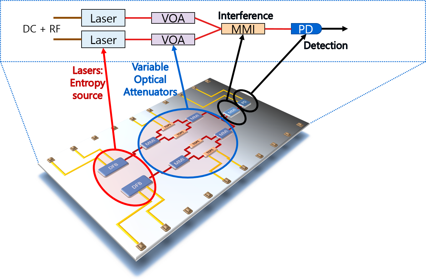
The novelty of our QRNG, as shown in this JOSA B paper, is in its plug-and-play format: as soon as it is assembled, it is ready to be used. All the optical components (the two lasers and a photodiode to detect the interfering pulses) are embedded onto a 6x2mm photonic chip, which is then connected to bespoke electronics. This is composed of an analog-to-digital converter reading the analog signal of the photodiode, and an FPGA that will post-process the data by removing any remaining information that an adversary can use. As an additional check, we ran the NIST test suite on subsets of our generated numbers, and observed that they passed all 17 tests. The output string of random numbers can then be used as input for the QKD modules.
A modulator-free quantum key distribution transmitter chip
The random key obtained from the QRNG is fed into a QKD transmitter. The transmitter chip developed by Toshiba removes the need for power-hungry phase modulators by the use of Master-Slave paired lasers. The information is encoded in the phase difference between pulses from the Slave laser, and can then be decoded by a receiving interferometer.
The working principle of the transmitter is based on combining the well-known phenomena of direct phase modulation and optical injection locking, both techniques already in use in classical optical communications. The idea of combining them for Quantum Communications was first introduced by Toshiba in 2016.
Direct phase modulation, as the name suggests, exploits the fact that the phase of a laser’s output is directly related to its driving signal: modulating such electrical current allows direct control over the phase of light emitted by a laser.
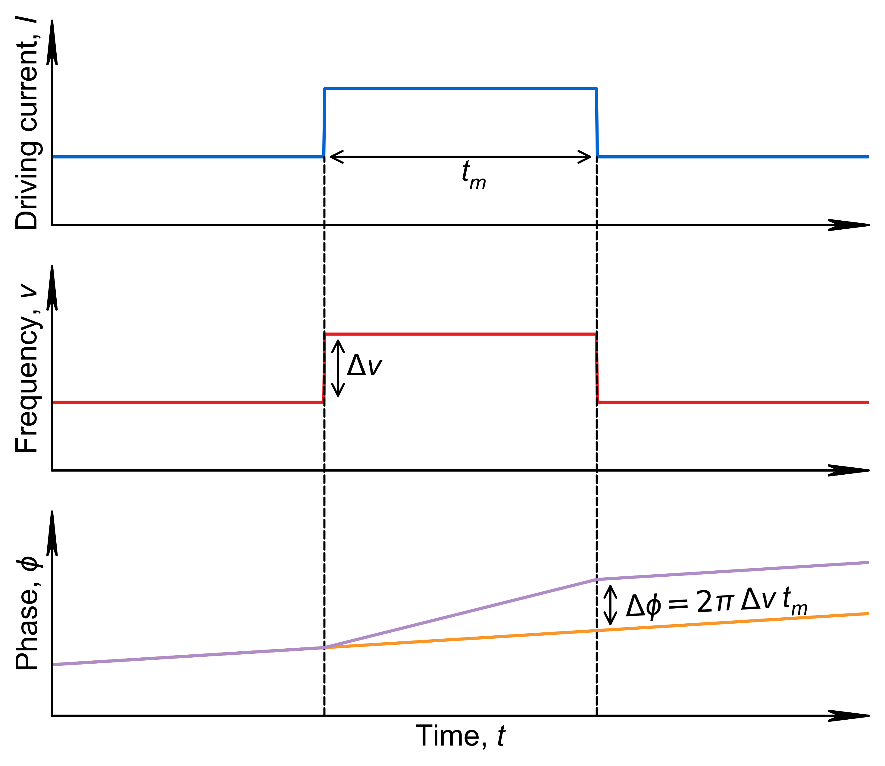
Optical injection locking is a phenomenon where one laser, namely the Master, injects light into a second, Slave, laser. This will cause the light from the Master to trigger emission from the Slave laser: light emitted from the Slave will then be “locked” to the same properties, in particular the same phase, as the injected light.
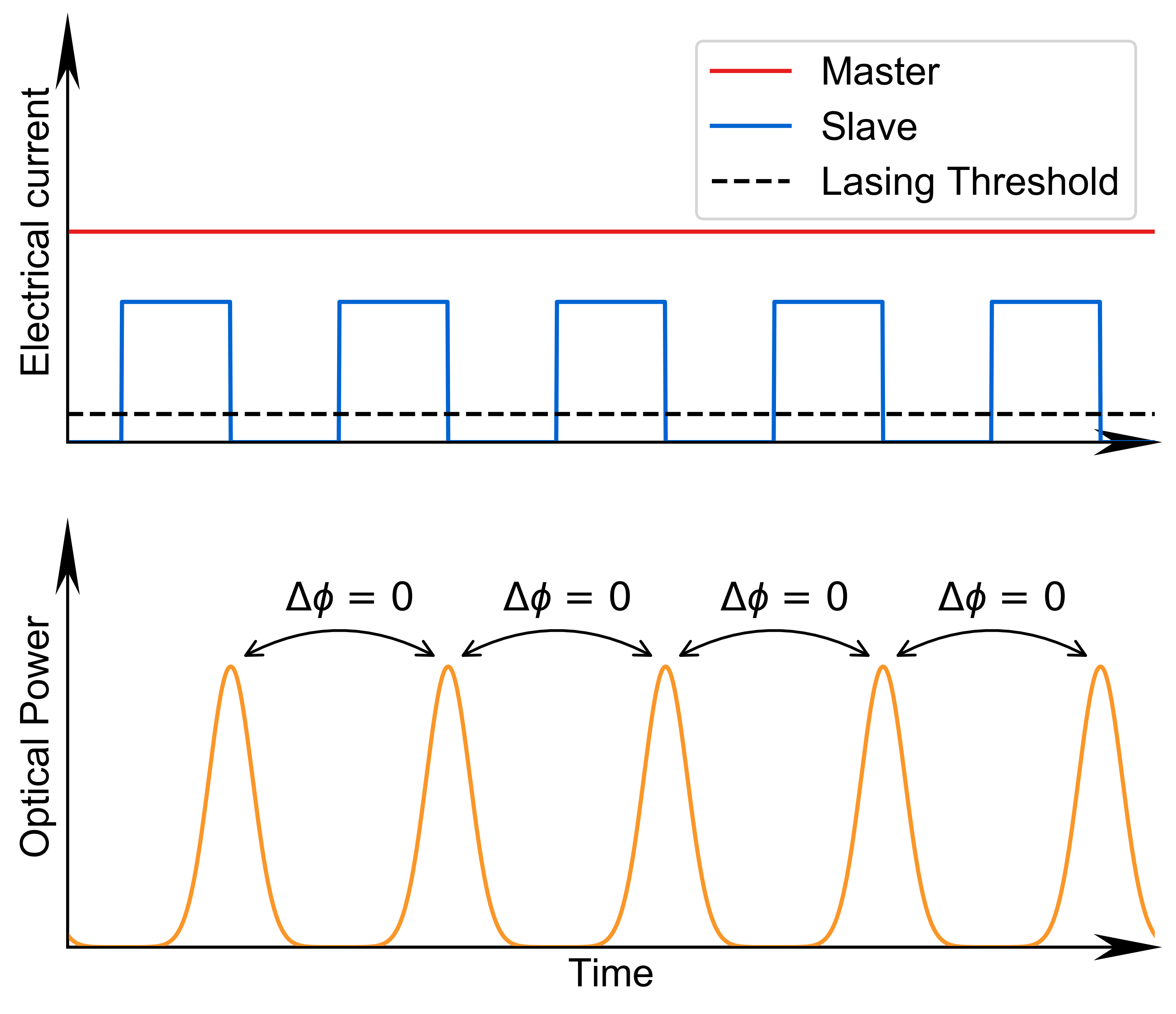
Combining these two techniques, we can then generate pulses from the Slave laser that will feature the phase we want to encode by modulating the Master.
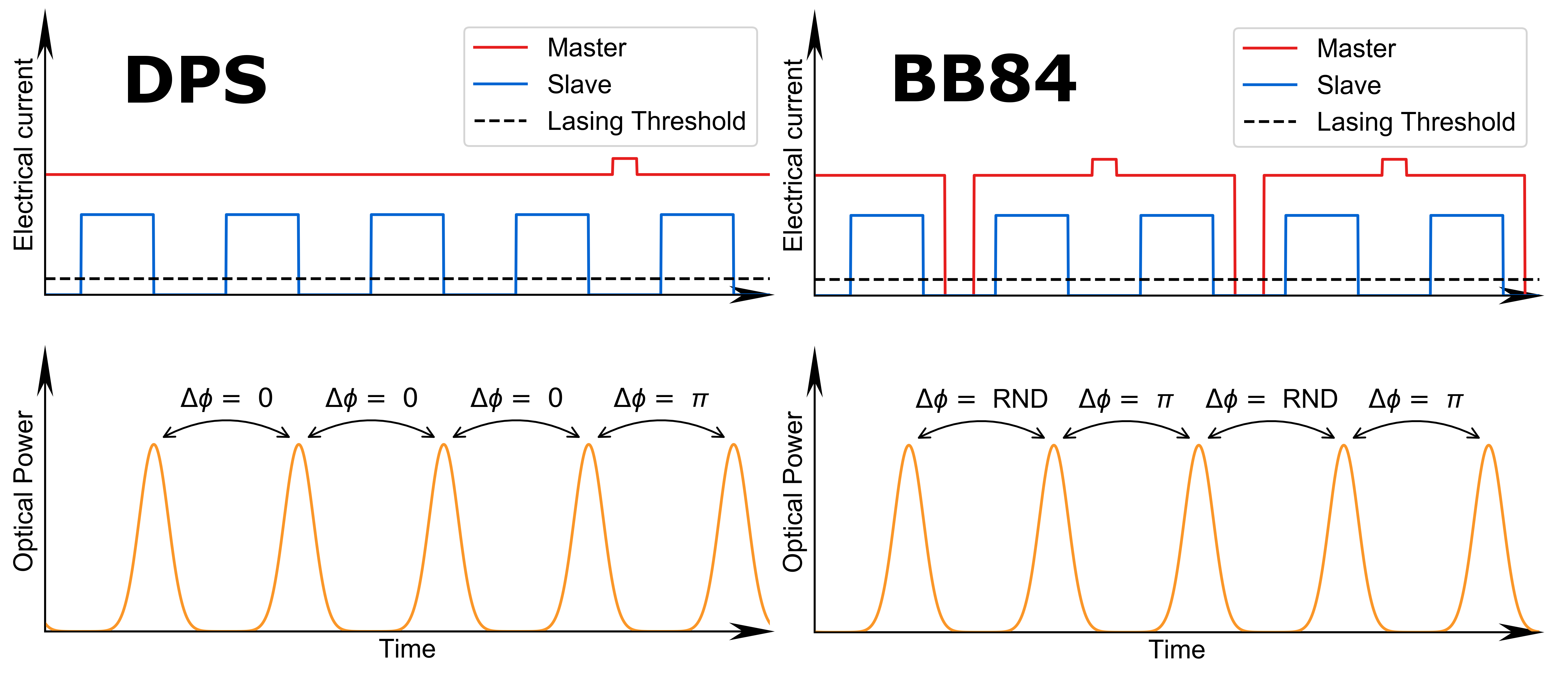
This removes the need for phase modulators, which are extremely power consuming, while still allowing us to encode all the relevant information in our photons.
Implementing this setup into a photonic chip results in a versatile, compact QKD transmitter. Our QKD chip was tested in an experiment that is described in this npj Quantum Information paper.
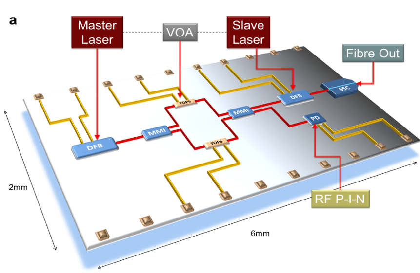
The simple layout of our device allows us to achieve results in line with state-of-the-art bulk implementations for both the BB84 and the DPS protocol.
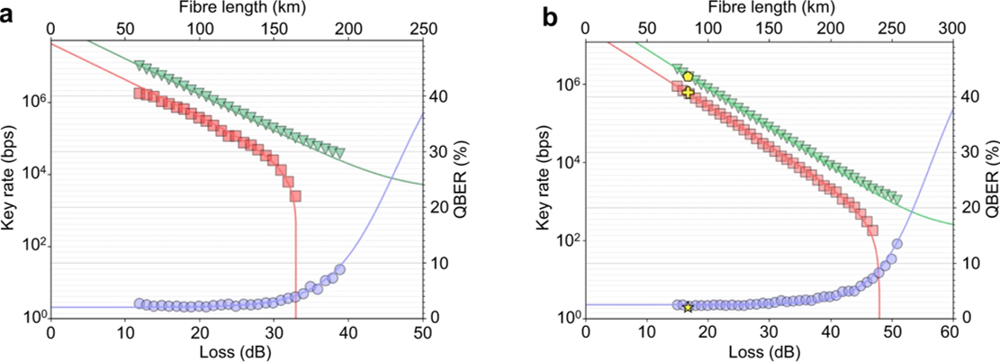
This shows that our devices are suitable for being implemented into QKD systems. The small form factor and the lower cost associated with the generic integration process, combined with the lack of phase modulators, make our QKD chips a candidate for large-scale implementation of Quantum Communication systems.
One thought on “Story of the month: Chip-based technologies for Quantum Communications”
Comments are closed.